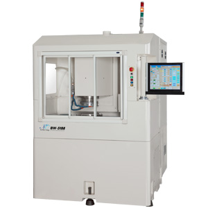
Feature
- Suitable for tape process
- Innovated, environment-friendly, energy-saving and efficient
- Successful applications in thickness reducing process for silicon wafers and GaAs
Patent
12 Patents in Taiwan and China
Advantages
- No need for solvent wash
- No need for wax on ∕ off process
- Lower cost and better production yield
Operation
The operator places the wafer attached to a flat ring + film on the platform of grinder to start manually parameter setting and thickness reduction. The semi-auto mode (i.e. automatic compensation) can be activated to measure wafer thickness and compensate to the defined target value both automatically until the thickness is reduced to target value.
Specifications
| Dimensions | 1440 mm × 1865 mm × 2440 mm ( W×D×H ) |
|---|---|
| Weight | 5050 kg |
| AC power | 3 Ø 220 V |
| Air supply | 5 Kgf ∕ cm2 ( 12 Ø Tube ) |
Object Wafer and Ring
| Wafer size | 2″~ 6″ |
|---|---|
| Chip size | None |
| Laser cut depth | None |
| Flat ring size | 10″ Flat Ring ( inner Ø 300 mm; outer 360 mm; t=1.0 ~ 1.3 mm ) |
Features
Moveable Operation Screen
Uniform Wafer Thickness After Grinding
Vertical Processing for Extra Rigidity
Colorful PC Touch Screen for Control Interface
Automatic Measurement of Wafer Thickness
The grinder and automatic measurement are combined in one unit for automatic measurement of wafer thickness
*The information provided here is for reference only. The actual specifications of equipment depend on the equipment requested and delivered.


