Feature
- Chip size 0.25~5.0 mm
- Apply to compound semiconductor SiC, GaN, InP
Advantages
- According to customer demand, break by different modes.
- Image auto-focus function
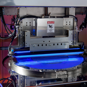
- Adjustable Large Hammer
- Auxiliary light on table
- CCD of imaging from top to bottom
Operation
Full Auto
Specifications
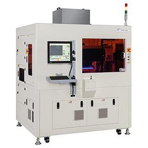
| Dimensions | 1790 × 1845 × 2332 mm ( W×D×H )(includes tricolored light) |
|---|---|
| Weight | 1550 kg |
| AC power | 1 Ø 220 V 50 ∕ 60HZ |
| Air supply | 5 Kgf ∕ cm2 |
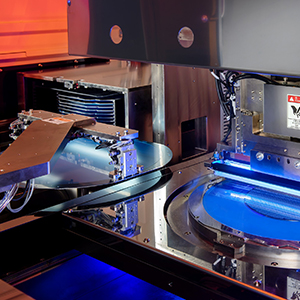
Object Wafer and Ring
| Wafer size | 2″~ 8″ |
|---|---|
| Ring Size | 12″ |
Features
Y-Axis Aligns Automatically
Set each cut or any cut to align once
θ-Axis Calibration and Y-Axis Alignment
Set each cut or any cut to align once
Patented Hold-Down Mechanism and Several Patented Breaking Modes
Wafers are held down to reduce wafer warping and improve production yield for breaking
Search Edge of Wafer Automatically
Search edge of wafer automatically and single X-axis alignment are provided for faster search
*The information provided here is for reference only. The actual specifications of equipment depend on the equipment requested and delivered.


