
Feature
- Chip size 0.25~5.0 mm
Advantages
- Fully automated protective film mounting and peeling solution for wafer breaking, significantly reducing manual operation time.
Operation
Full Auto
Specifications
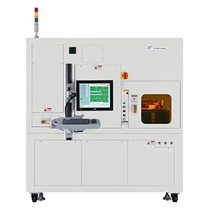
| Dimension | 1860 mm × 2544 mm × 2334 mm ( W×D×H )( including tricolored light ) |
|---|---|
| Weight | 2570 kg |
| AC Power | 11 kW 3Ø5 W 400 V / 220 V |
| Air Supply | 5~7 bar |
| Vacuum Supply | -1 ~ -0.8 bar |
Object Wafer and Ring
| Wafer Size | Diameter: 2-inch ~ 8-inch Thickness: ≤ 300 μm |
|---|---|
| Chip size | 0.25~5.0 mm ( The practical application depends on the laser cutting quality and the properties of the wafer material. ) |
| Wafer | 12-inch Flat Ring |
| Tape Size | 240 mm x 100 M ( Total length of one release film roll ) |
| Tape Material | PET |
| Tape Thickness | 25μm ~ 50μm ( 0.025~0.05 mm ) |
Features
Compatible with different wafer sizes
2-inch / 4-inch / 6-inch / 8-inch / Broken Wafer
Floating pressing mechanism
IR ∕ B light source
Top CCD
CCD of imaging from top to bottom
Image auto-focus function
Automatically achieves clear imaging for different product thicknesses during automatic image search, preventing errors caused by focus deviation.
CCD of Detecting Full ∕ Broken Wafer
CCD automatic identification of full/partial workpieces with automatic parameter and breaking mode selection.
Auxiliary light on table
Improve image capture yield under different surface conditions.
Adjustable Large Hammer
Adjustable using number of hammers, hitting times, and impact force.
Dice Holding Mechanism
Prevent displacement after wafer breaking with small dies.
Protective film mounting
Mount protective film before wafer breaking.
Protective film peeling
Peel off protective film after wafer breaking.
Waste film collection
Dedicated waste film tank for collecting peeled-off protective film.
PC / PLC
User-friendly touch screen; advanced image processing system.


*The information provided here is for reference only. The actual specifications of equipment depend on the equipment requested and delivered.